There seems to be a little confusion concerning the true effects of cathode bypass on low frequency amplifier performance. The truth is, gain benefits from cathode bypass are limited. And not by capacitor size, but by the basic design of the amplifier stage.
Normally when one looks at coupling (i.e. dc blocking) capacitors between stages, the effects of low frequency rolloff are cumulative the lower the frequency goes. In this case gain falls off at ≈20dB per decade of frequency or by ≈6dB per octave. And it doesn’t matter how far down in frequency one goes. The rolloff continues.
However, in the case of cathode bypass capacitors this relationship does not hold. And the reason for this is simple. The cathode bypass capacitor is not a simple pole in the gain function of the amplifier. It is instead, a pole in the cathode feedback function of the individual stage. The only effect a cathode bypass capacitor has on the amplifier is in the operation of the individual amplification stage. And this function is not to attenuate signal, but to modify how the amplification stage actually functions.
To illustrate this phenomenon I decided to work through a real world example. I chose the driver stage from the 6V6 Marblewood amplifier. For reference, this driver is really just the same as the Universal Preamp with one critical difference. In the Marblewood, the stage is loaded by the 470kΩ grid resistor of the power stage. In the Universal Preamp, it is loaded by the 250kΩ output potentiometer. As we’ll see later, this makes a measurable difference in how the cathode bypass capacitor actually functions in the circuit. As a reminder, here is the schematic for the Marblewood.
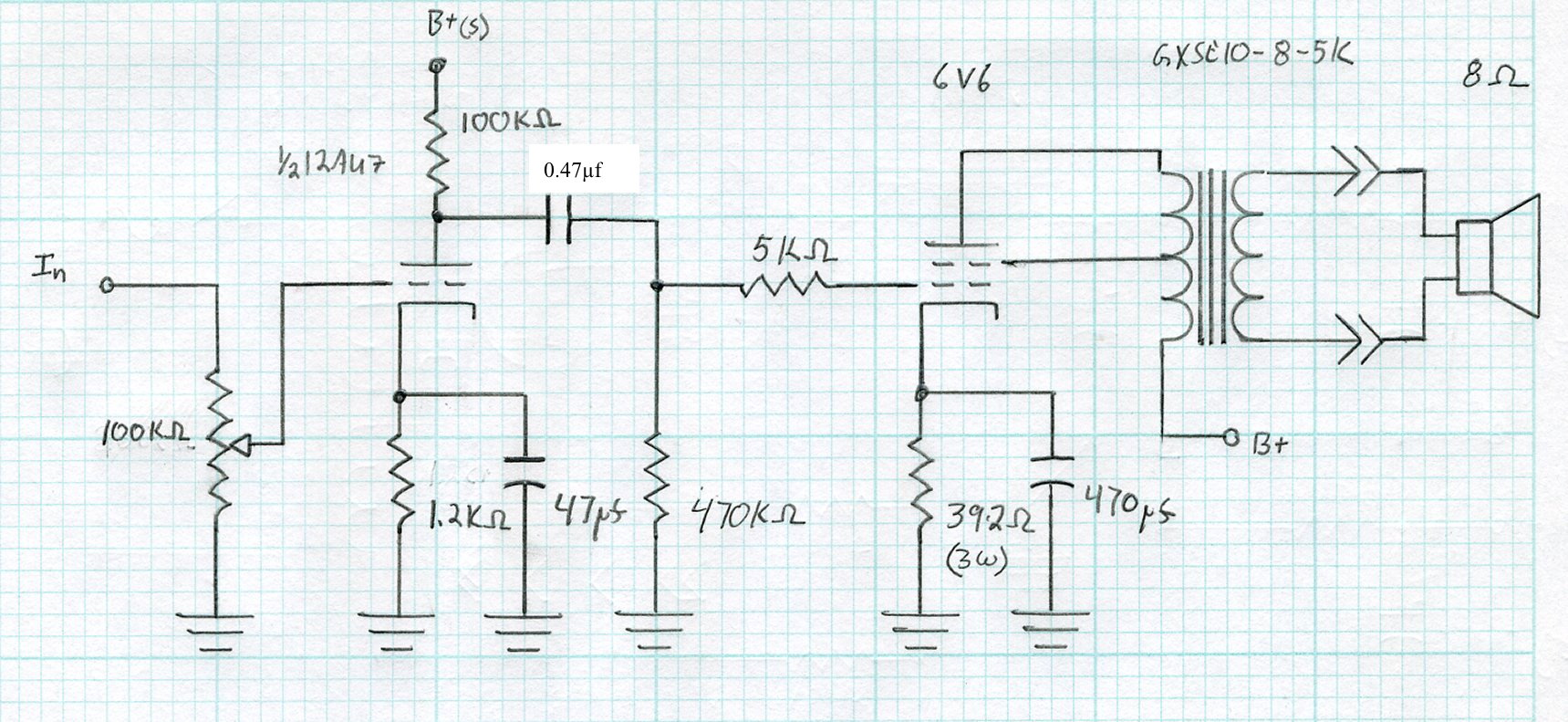
Focusing on the driver, the plate load is 100kΩ, the cathode load (i.e. the cathode bias resistor) is 1200Ω, cathode bypass capacitor is 47µf, the grid resistor for the follow on stage is 470kΩ, and the coupling capacitor is 0.47µf. The goal is to determine exactly how the cathode bypass capacitor affects the driver operation across frequency.
The first step is to examine the load line design I used to get to this design. Below I have included the load line design sheet showing the functional data overlaid on the 12AU7 plate characteristics curves.
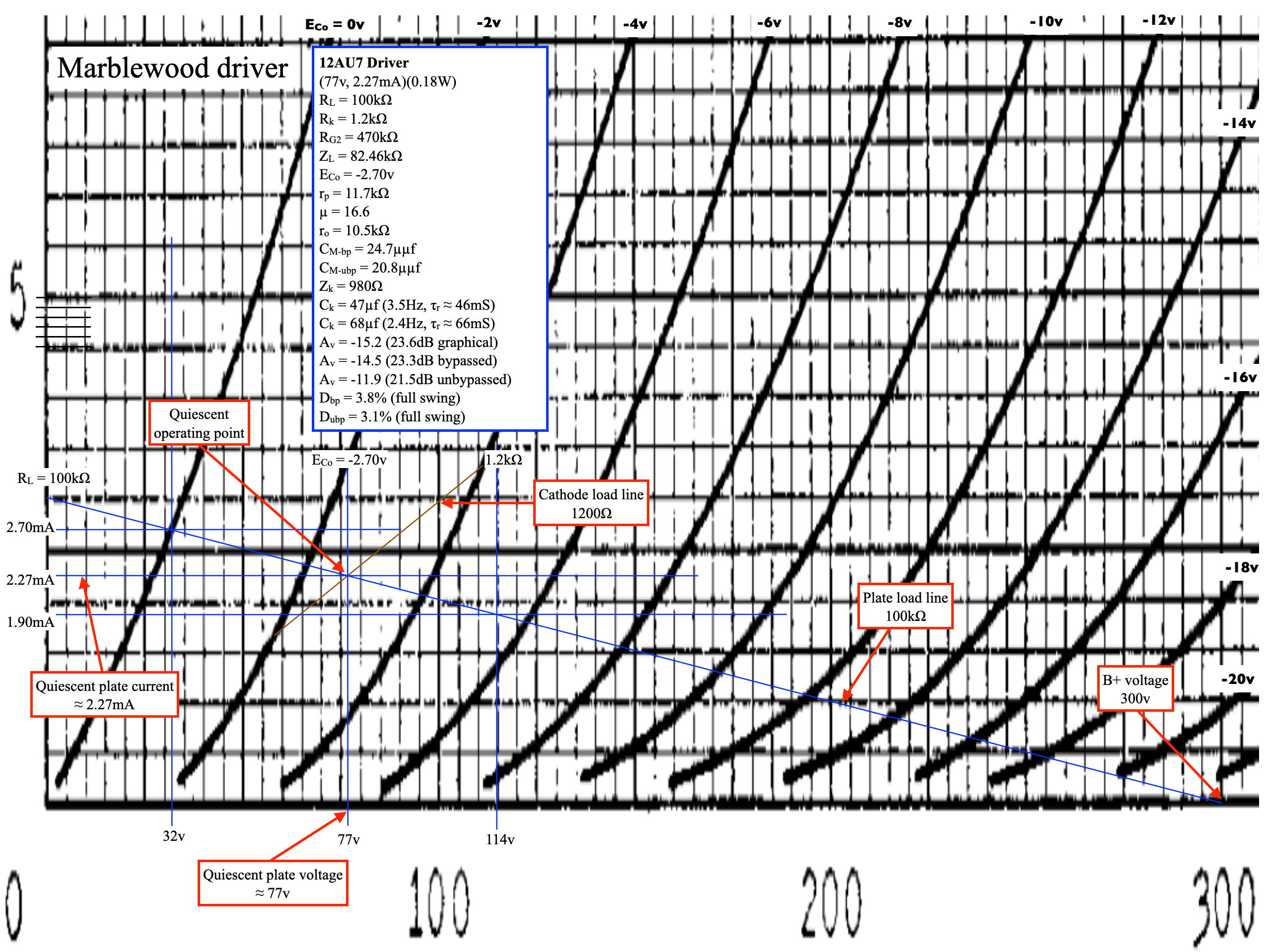
I have added some labeling to illustrate the important points of the graphical design. The data in the box contains both the relevant circuit parameters as well as the calculated performance results for the stage. But before reviewing the calculations, there are two additional pieces of information needed from the 12AU7 data sheet. These are the tube factors µ and rp (i.e. amplification factor and plate resistance) at the design operating point. The easiest way to determine these is directly off the graphs provided in the data sheet.
Using the operating point determined from the graphical load line, the tube factors are read directly off the graph shown below.
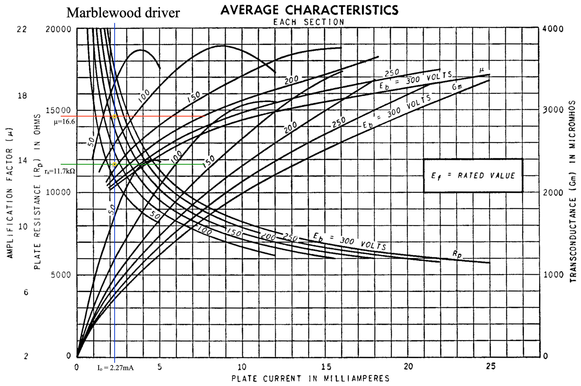
Here I have drawn a vertical line at the quiescent operating current through the curves for µ and Rp. Then I have used the quiescent plate voltage to interpolate between the appropriate curves to find the exact values to use. From the above graph, µ=16.6 v/v and the plate resistance is ≈11.7kΩ.
Returning to the load line, there is significant information in the data box. Working from top down you’ll see the various circuit factors and then, six lines down is an impedance labeled Zl. This is the AC load impedance on the plate lead. It is simply the parallel combination of the plate load resistor (100kΩ in this case) and the next stage grid resistor (470kΩ in this case). The 100kΩ in parallel with the 470kΩ is ≈82.46kΩ.
This is why I said that the difference between this driver and the universal preamp was important. If the 100kΩ plate load was in parallel with the 250kΩ potentiometer from the universal preamp, then Zl would be ≈71.43kΩ and the stage would behave differently.
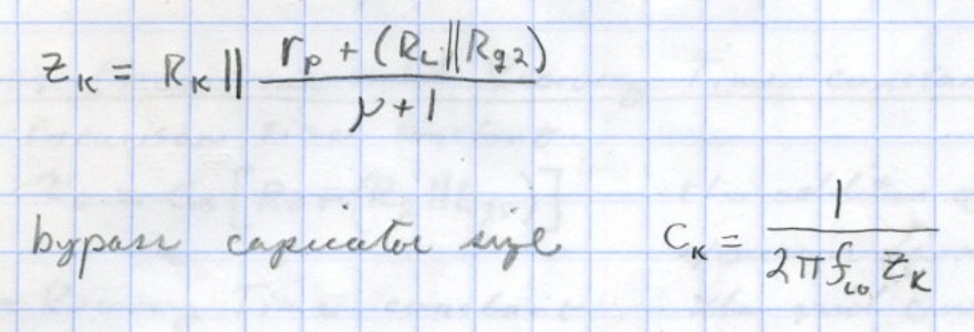
The next important item I would like to point out is the impedance labeled Zk. This is the cathode impedance. This is the total impedance seen by the cathode bypass capacitor. It is the parallel combination of the 1200Ω cathode resistor and the impedance seen “looking into” the cathode pin of the tube. Here is the equation for calculating this impedance from my notebook.
Please ignore my bad spelling. 🙂
From this relation the cathode impedance of the tube is just the series combination of the plate resistance and the total AC plate load of the circuit all divided by µ+1. The reduction by µ+1 is because any change in current through the tube (via the voltage difference between the grid and cathode pins) is amplified by µ+1 through the anode load. Therefore, the plate load looks smaller, as seen from the cathode, by the amount µ+1. Using the values from the load line design Zl ≈ 980Ω ≈ 1200Ω || (11.7kΩ + 82.46kΩ)/17.6. Also included above is the relation for finding the transition frequency due to the cathode bypass. We’ll come back to this relation a little later.
Moving down the list the astute reader will notice that there are three different values listed for the voltage amplification of the driver. The first is derived graphically from the load line. This is the least accurate way to determine stage gain but is handy if exact values for µ and rp cannot be found. But it is the two additional values that are of interest here. The difference between these two gain values is simply the presence or absence of a cathode bypass capacitor. These are labeled “bypassed” and “unbypassed”. The relations to find these two amplifications, also from my design notebook, are shown below.
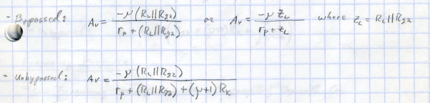
The difference between these two relations is informative. In the bypassed case, the total amplification factor of the tube is simply reduced by the voltage divider relation Zl/(rp + Zl). However, in the unbypassed case something else happens. Because there is no low impedance path for AC signals to bypass the cathode resistor, fluctuations in current cause fluctuations in the apparent grid voltage (derived by the current flowing through the cathode resistor). This serves to reduce the gain by an additional series impedance in the voltage divider relation, (µ+1)Rk. This reduction in amplification is what is meant by the term “cathode degeneration” used in much tube design literature.
Returning to the Marblewood driver, using the values already found, the two values for amplification are found as -14.5 v/v and -11.9 v/v (negative because the stage is inverting). In decibels, 23.3dB and 21.5dB. This is an important finding with relation to the cathode bypass capacitor. With no capacitor present (or a very small capacitance) the driver will have a gain of 21.5dB. With the largest capacitor possible in place, the driver will only have a gain of 23.3dB. The maximum difference in gain due to cathode bypass, at any frequency, is only ≈1.8dB. And this illustrates the limitation in the ability of cathode bypass to affect low frequency performance.
To illustrate how this affects stage gain across frequency, I put together a spread sheet to calculate some curves. Before getting to the curves, here are the scalar calculations from the simulation.
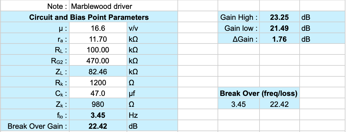
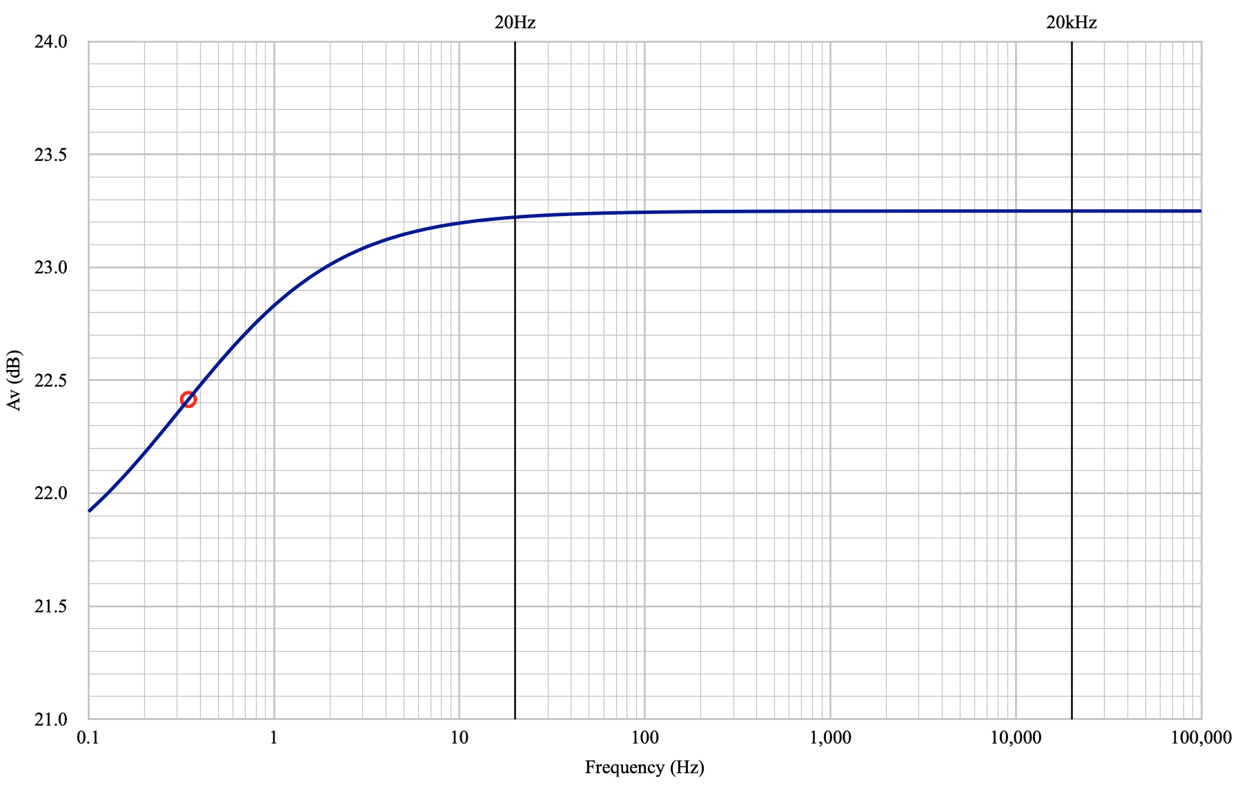
The white boxes are inputs and the blue shaded boxes are the results using the relations discussed above. The transition frequency, flo, is calculated from the relation above for bypass capacitor size (from my design notebook) simply solved for frequency and using the 47µf capacitor from the design. The “Gain high” and “Gain low” numbers are, as indicated above, limits on performance. The gain high being at “high” frequency (i.e. cathode bypassed) and “gain low” being at low frequency (i.e. cathode unbypassed). It is informative to see how this looks in the transition frequency region. Below is a plot of the theoretical gain change for the driver from very low (0.1Hz) to very high (100kHz) frequency.
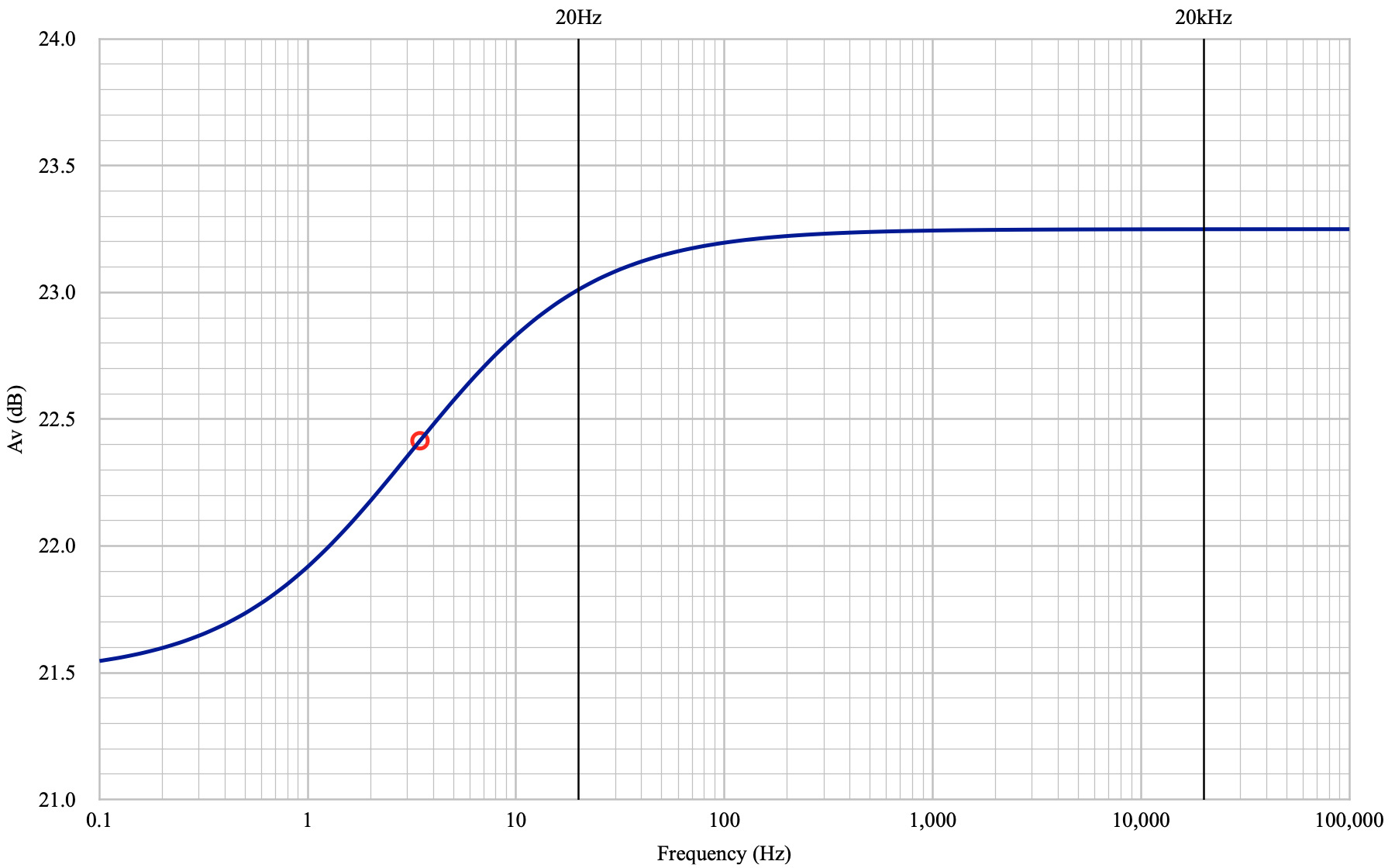
The limits of the curve clearly show the gain has topped out at 23.25dB at the highest frequency and is asymptotically approaching 21.49dB at the lowest frequency. But at the “transition frequency” the gain falloff is not 3dB as it would be for an interstage coupling capacitor, but is only down by ≈0.83dB.
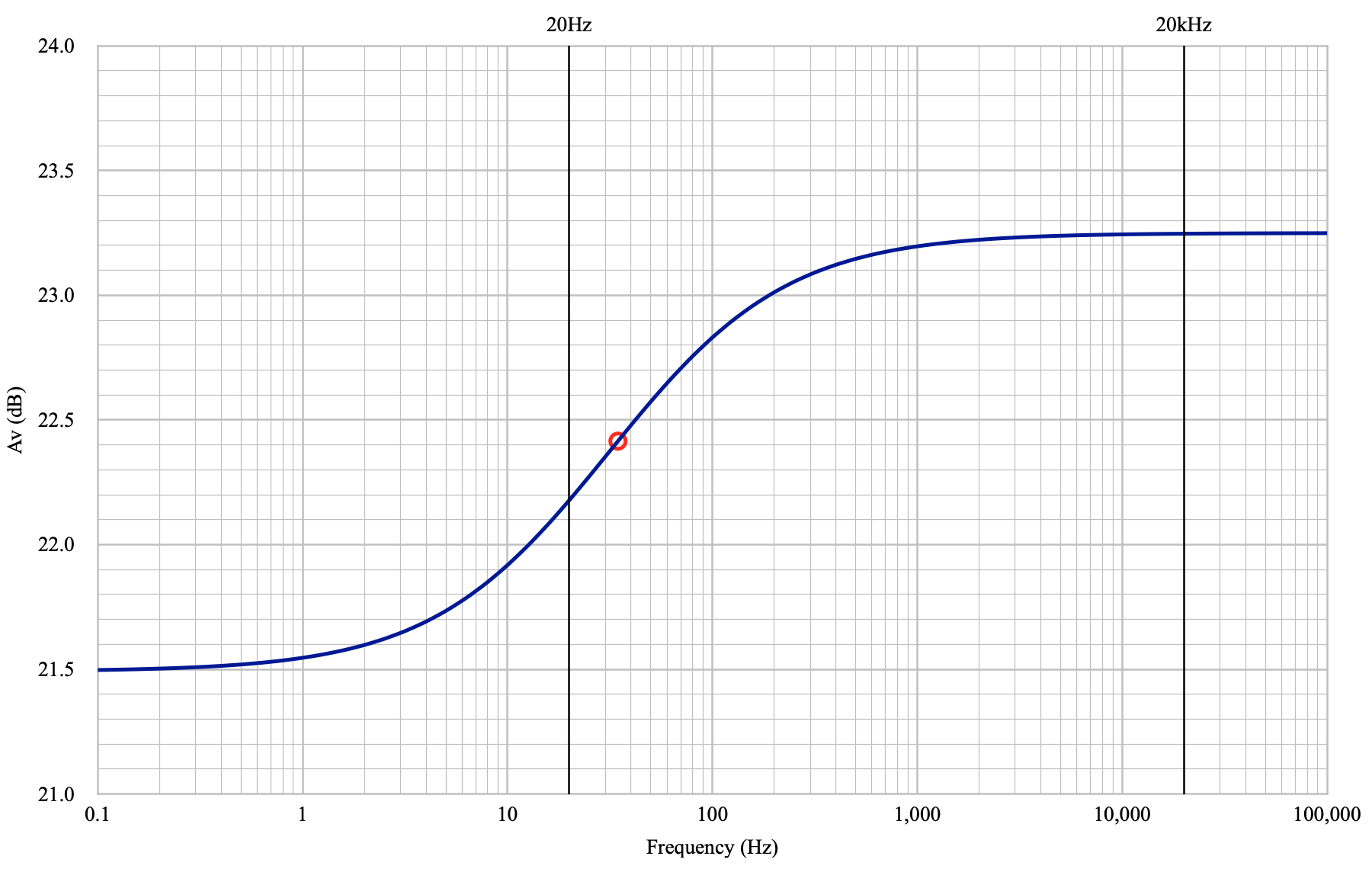
I have highlighted the lines for the assumed bandwidth of the stage on the plot. As can be seen at 20Hz, the loss is actually very minimal. Only 0.24dB in this case. The lesson here is that even making the bypass capacitor very large, there is very limited advantage to be achieved in low frequency amplification. In fact, it’s informative to repeat the plot above, but with a ten times larger bypass capacitor of 470µf. Here is how that looks.
In this case, the “transition frequency” has been reduced from 3.45Hz to 0.35Hz, a full decade of reduction, but the loss at 20Hz has only been reduced from 0.24dB to 0.03dB. This difference, 0.21dB, is impossible to differentiate with the human ear regardless of the test conditions or methodology.
It is also interesting to see what happens if the bypass capacitor is reduced instead of increased. I decided to generate the plot with a ten times smaller bypass capacitor of only 4.7µf. Here’s how that plot looks.
In this case, the transition frequency has been increased to 34.5Hz from 3.5Hz, this time an increase of a full decade. However, the loss at 20Hz has only increased to 1.07dB. So even with what most would consider a very small bypass capacitor, the falloff at 20Hz is not catastrophic.
The primary finding from all of this is that there is little to be gained from overly large cathode bypass capacitor size in relation to low frequency performance. However, I will add that there can be catastrophic consequences to transient overload performance if the capacitor is too large. And it’s for this reason that I am always careful to never make these bypass capacitors any larger than they need to be.
I will also mention that the overall value of the AC load will affect this situation. As the value of Zl gets smaller, either from a smaller plate load resistor or a smaller input resistance on the following stage, then the difference between the upper and lower limit can increase. This will then affect how much falloff occurs at the transition point and whatever low frequency performance point is of interest (e.g. 20Hz, 30Hz, etc.). If anyone would like to see some examples of this phenomenon, changing delta-gain with variations in Zl, just let me know.
I am hopeful that this simple example will help to clear up some of the confusion surrounding cathode bypass capacitors and their effects on overall frequency performance.
As always, questions and comments are welcome.
The plots at the end are an excellent aid in the understanding of this theory. Thanks.
You’re welcome. I’m glad that someone found the information of some use.
Pingback: Cathode Bypass and Frequency Range, Part II | Cascade Tubes