In my last post I threw in a comment at the end pointing out that lowering plate load resistance will play a part in how the cathode bypass capacitor behaves. Someone asked, so I thought an example of how this affects things might be in order.
For this example I chose to use the driver stage out of the “Color Preamp” but with a simple 470kΩ resistance on the following stage (instead of the cathode follower). For this example I used the same basic circuit but used four different values of plate load resistor (47kΩ, 68kΩ, 100kΩ, and 200kΩ) to help illustrate the differences.
First, let me present the four load lines for these different plate loads.
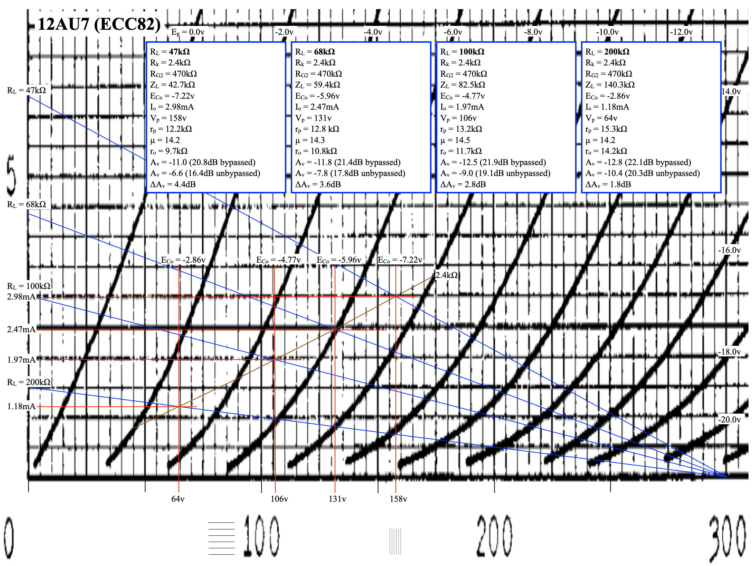
The values for plate resistance (rp) and amplification factor (µ) were found in the same way as the last post. I have also included a line in the data boxes for ΔAv. As can be seen in the figure, as the plate load decreases, the change in gain between bypassed and unbypassed cathode operation increases. At the highest load the delta is ≈1.8dB whereas at the lowest load the difference is ≈4.4dB. Note that this difference has nothing to do with the size of the bypass capacitor. It is entirely due to the operating point of the stage and the effects of the plate load resistance. The bypass capacitor size only affects the frequency at which the transition will take place.
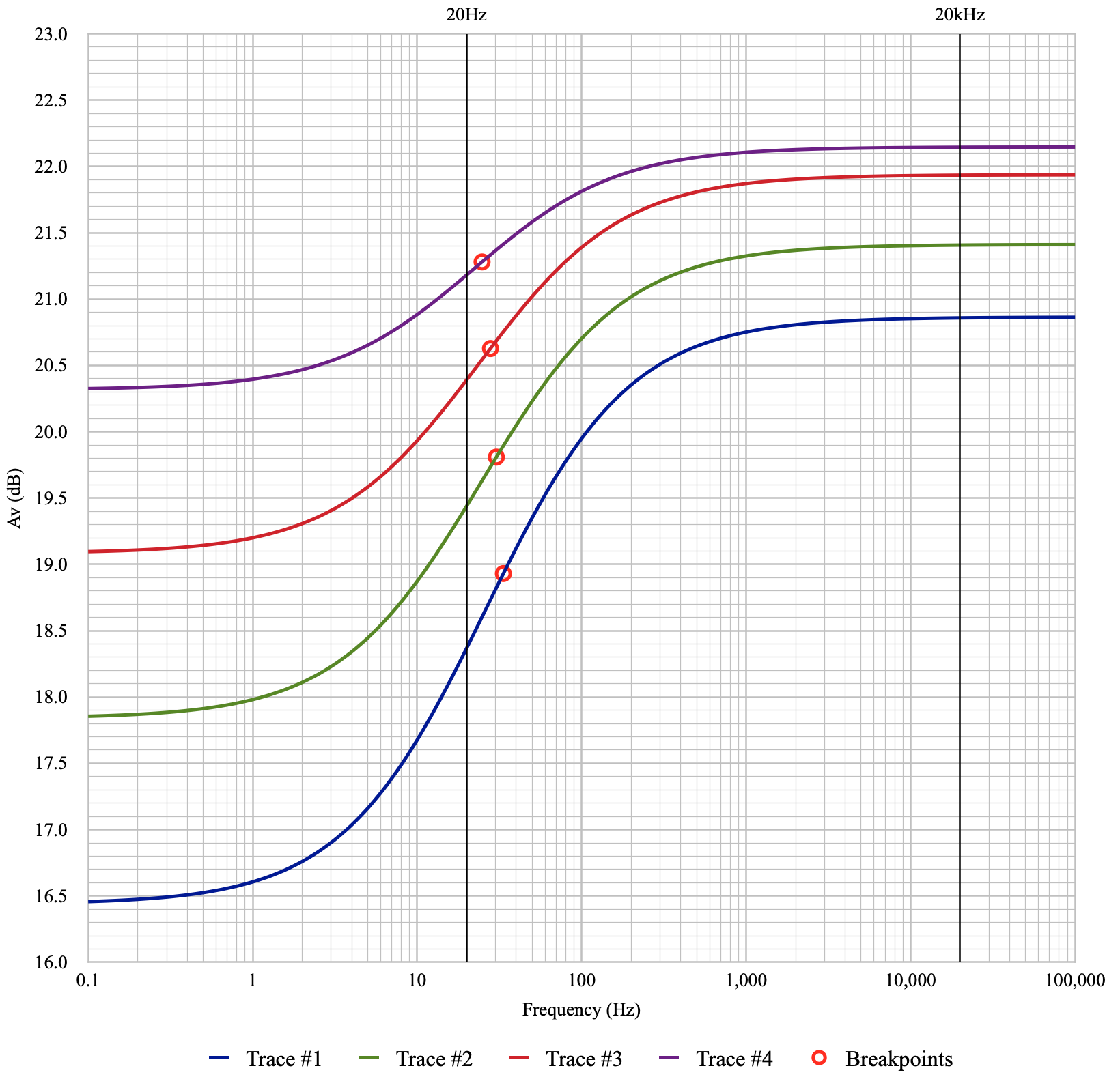
Just like the last post, I generated some curves showing how gain changes with frequency. Only this time I have overlaid the four curves to highlight the differences. Before I show the curves, here are the simulation inputs for each curve.
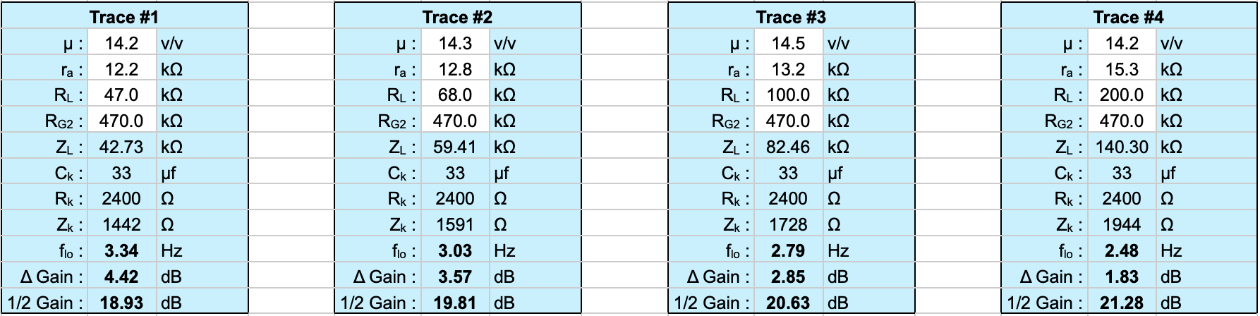
All four of these cases use the same 33µf cathode bypass capacitor and next stage grid resistor. All that changes is the value of the plate load resistor. Here are the curves.
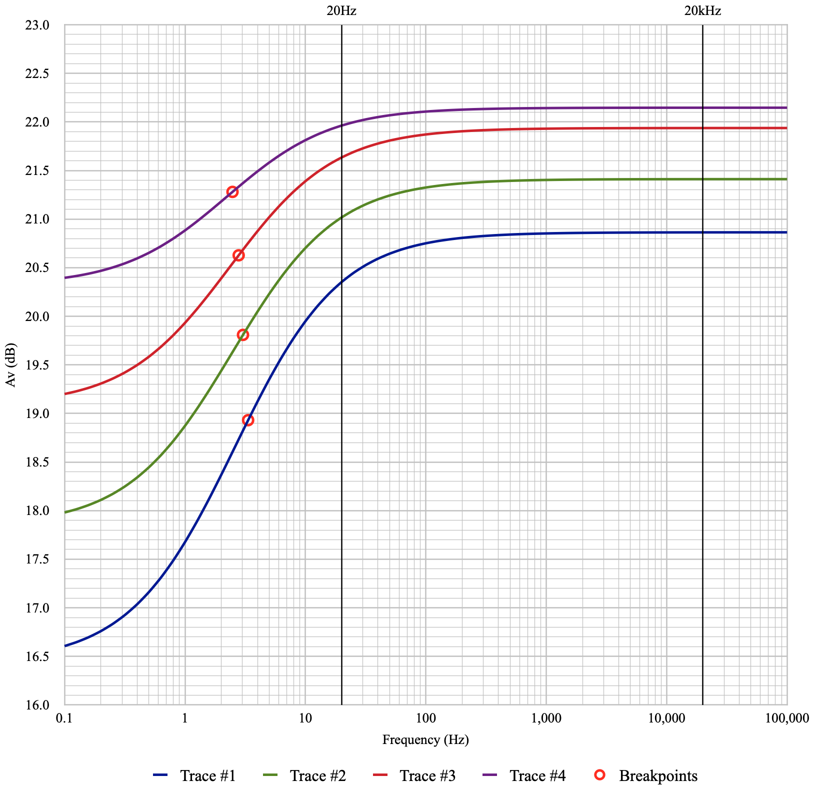
This plot illustrates how the different stages behave across frequency. A the higher frequencies there is about 1.3dB difference in overall gain between the four cases. However, as frequency drop those differences become more apparent. Looking at the losses at 20Hz, the losses due to cathode bypass are 0.51dB, 0.40dB, 0.30dB, and 0.18dB respectively for traces #1 through #4. Normally, I would consider the 0.18dB loss a reasonable design point for a single stage, but I would be more reluctant to accept the 0.51dB loss. For this design I would likely opt for a lager bypass capacitor like a 47µf instead of the 33µf used to generate the curves above.
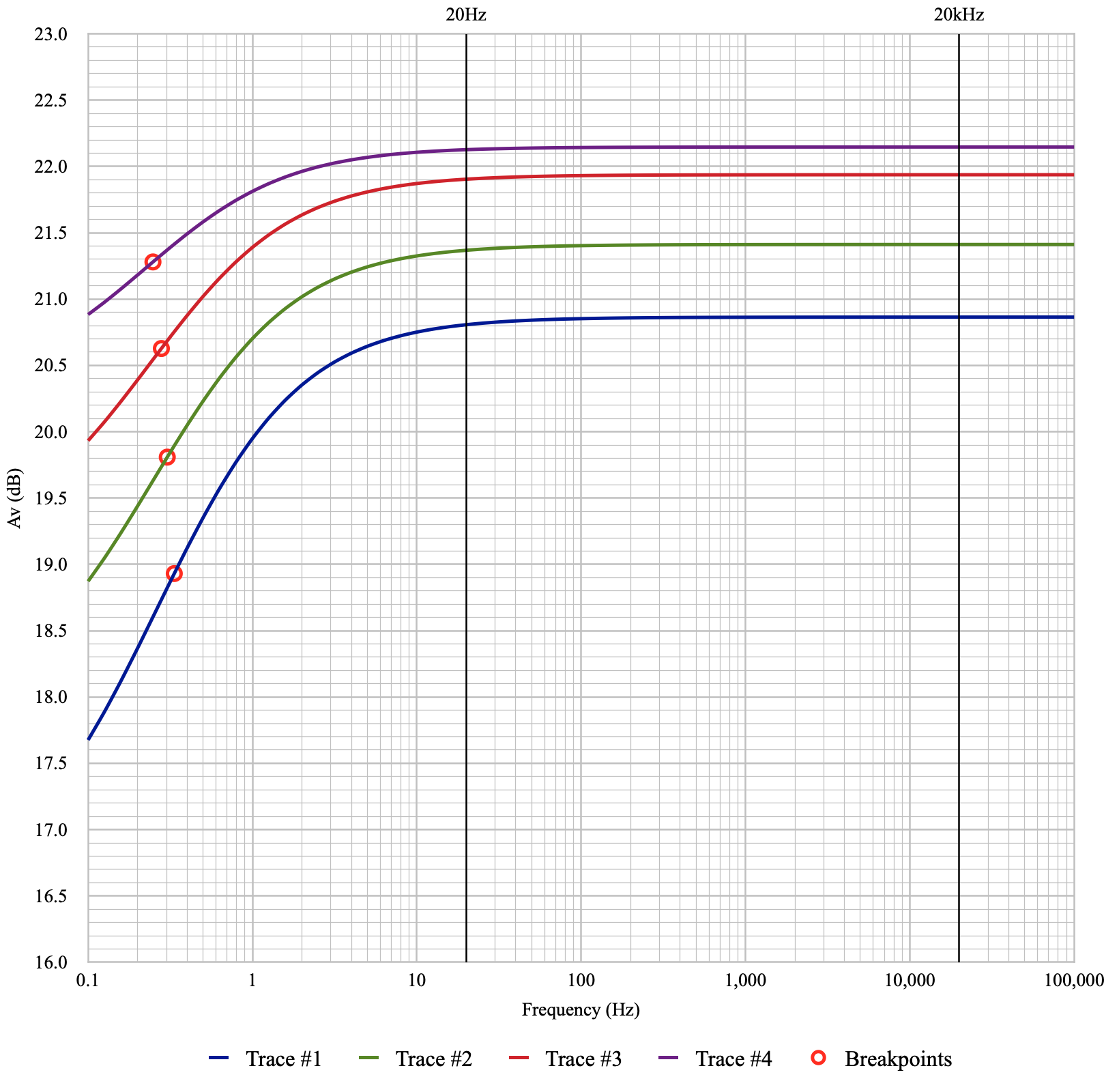
It is illustrative to see how changes in the bypass capacitor size affect this performance. Reducing the bypass capacitor size by a factor of ten shows the effects of plate load variation more clearly. Here are the same four traces but with a 3.3µf bypass capacitor.
In this case the losses at 20Hz have increased to 2.50dB, 1.97dB, 1.55dB, and 0.97dB respectively for traces #1 through #4. In this case with the highest plate load resistance, the falloff in bass response in combination with other amplifier responses may not even be noticeable at ≈1dB. However, adding 2.5dB to the low end rolloff in a single stage would likely be unacceptable. Again note that the change between these two cases is not the size of the bypass capacitor but rather the change in the plate load resistor.
By going the other way in terms of bypass capacitor size and increasing it, the differences may be minimized. However an over sized bypass capacitor can lead to other performance issues. Here are the four curves repeated with the bypass capacitor increased by a factor of ten to 330µf.
In this case the losses at 20Hz have been reduced to 0.06dB, 0.04dB, 0.03dB, and 0.02dB respectively for traces #1 through #4. These are all acceptable gain falloff numbers, but in every case the over large bypass capacitor will lead to serious overdrive recovery problems.
It is easy to get a biased view of the magnitude of these effects when looking at these plots. On the three plots above the entire y-axis extent is only 7dB. A better feel for the overall effects can be seen by showing the bandwidth effects of not only the bypass capacitor, but the coupling capacitor and follow on stage as well.
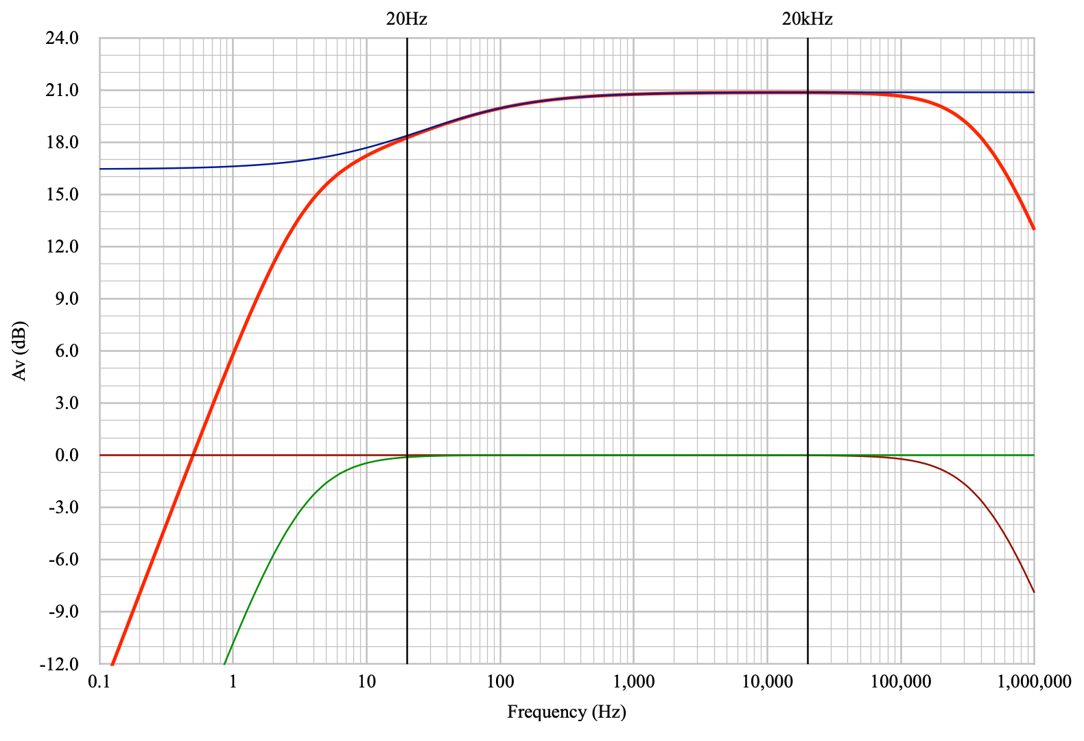
To illustrate this I have constructed a bandwidth plot with individual curves showing the effects of cathode bypass, coupling capacitor size, and follow on stage Miller capacitance. Having all three curves on the same plot helps to make more realistic comparisons of the individual effects. The following are the input parameters for the 47kΩ plate load case.
I have chosen a coupling capacitor size which yields small (≈0.12dB) loss at 20Hz. I have an assumed Miller capacitance of the follow on stage of 25µµf and have employed a 5kΩ grid stopper resistor on the follow on stage. This configuration yields for following bandwidth plot.
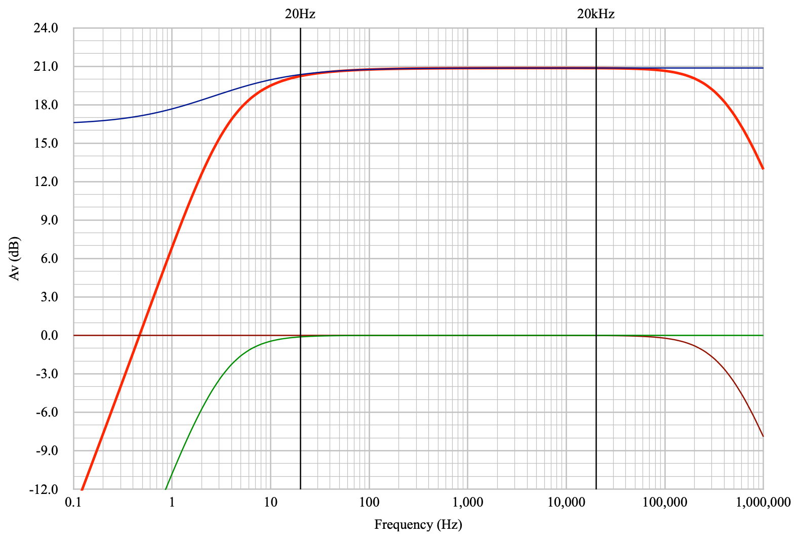
In this plot, the blue line represents the falloff due to the bypass capacitor. The green curve is the falloff due to the coupling capacitor, and the brown curve is the falloff due to the Miller capacitance of the following stage. The heaver red curve is the combined bandpass response of the stage. In this case, the falloff at 20Hz is ≈0.63dB. I would say this this represents an appropriately sized bypass capacitor. However, increasing the bypass capacitor to 47µf reduces the falloff at 20Hz to ≈0.49dB. It would be arguable if the additional 0.14dB of gain at 20Hz would be worth such a change.
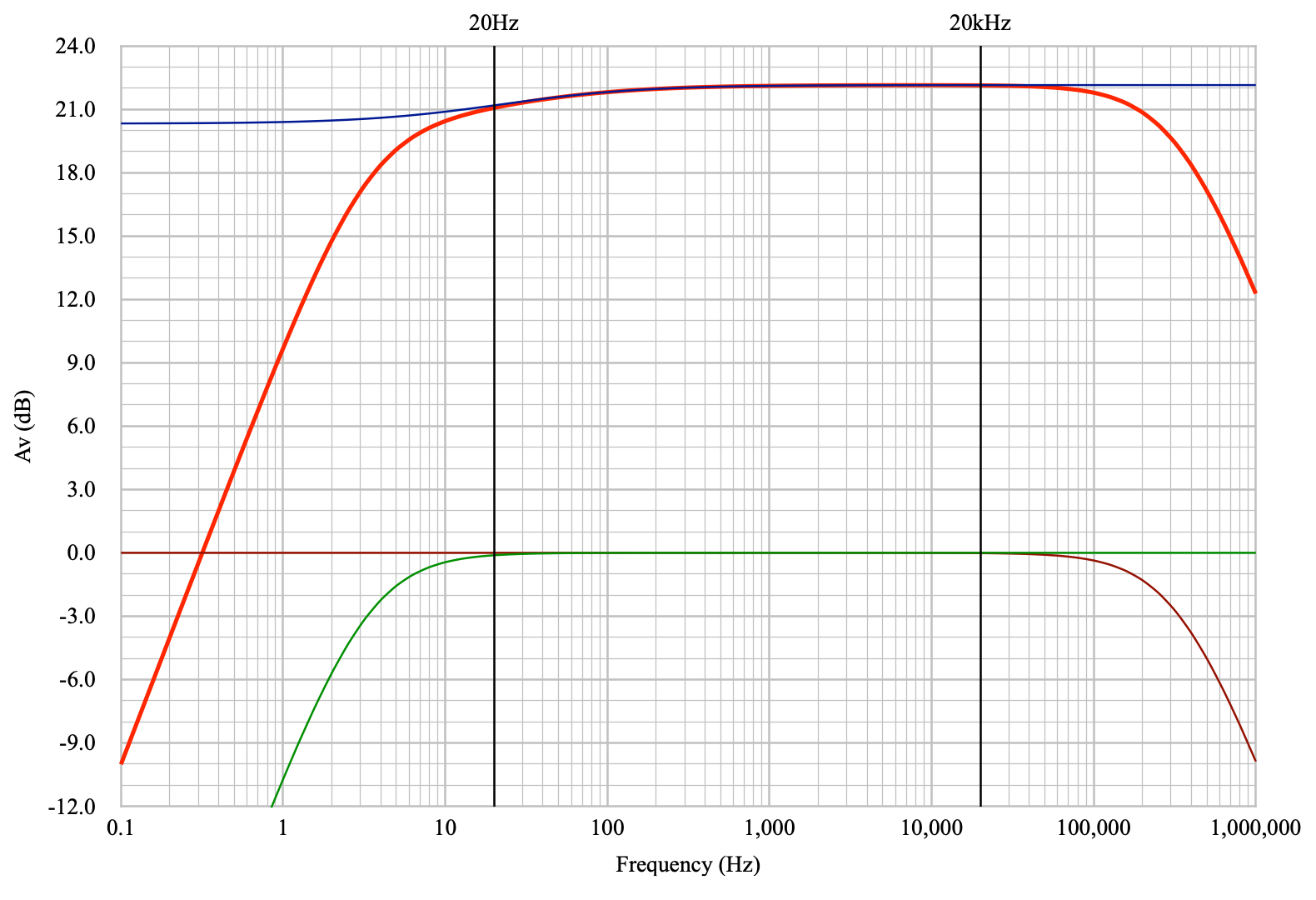
To illustrate the problem of a too small bypass capacitor, I regenerated the bandpass characteristics but with the bypass capacitor decreased by a factor of ten to 3.3µf. These curves should illustrate the relative differences resulting in the overall bandpass characteristic.
In this case, the effect of the bypass capacitor on the overall bandpass characteristic is clearly evident. Here the fall off at 20Hz is ≈2.6dB. Note that increasing the coupling capacitor size will not markedly improve this situation. This falloff is almost entirely due to the undersized cathode bypass capacitor.
It is also informative to see what happens if the plate load resistor on the stage is increased with nothing else changing. Here is the same stage, with the undersized 3.3µf bypass capacitor, but with the plate load resistor increased to 200kΩ.
Here the loss at 20Hz has been reduced to ≈1.07dB with no changes to the bypass capacitor. This change, an improvement in 20Hz rolloff of ≈1.53dB, is solely due to the differences in bypassed verses unbypassed gain in the stages with different plate load resistances. And in this stage, with the 200kΩ plate load, an increase of the bypass capacitor from 3.3µf to 22µf reduces the falloff at 20Hz to only ≈0.38dB.
The overall point to take from all this is that seldom do individual component values dictate the entire situation. Differences in how a stage operates due to one component choice, will have an effect on how other component changes affect the overall performance. And sometimes there may be a reason for stage performance anomalies that are not apparent at first.
I hope that this discussion, in conjunction with my last post, helps to shed some light on how cathode bypass capacitors affect overall stage performance.
As always, questions and comments are welcome.
I have just come by your website today and am thrilled with what I see! I will be coming back on a regular basis from now on. I have been involved with DIY audio for over 20 years now and have been building my amplifiers since that time. I am still learning and have learned new things as I have read the cathode bypass info. BTW is the best bypass no bypass as far as frequency is concerned?
From a frequency perspective, yes, no bypass will maximize the width of the bandpass characteristic. Including going down to DC on the low frequency end. However, that cathode degeneration is an application of negative feedback and will (at least in my opinion) harm the harmonic structure of the stage response.
So the question of bypass being good or bad really falls on the requirements of what you’re trying to achieve with the amplifier stage design.